How the Advanced Ozone Cleaning Process Improves Wafer Yields and Reduces Costs

How the Advanced Ozone Cleaning Process Improves Wafer Yields and Reduces CostsEditor’s Note: This article was originally published in January 2017 and has been updated with additional information and reposted in April 2023.

Modutek’s advanced ozone cleaning is a highly effective method for removing contaminants from wafers. The process involves using ozone gas, which is a highly reactive oxidant, to break down and remove organic and inorganic contaminants from the surface of the wafer. The process is typically performed in a closed chamber that is designed to contain and recirculate the ozone gas.

How Advanced Ozone Cleaning Works

The advanced ozone-cleaning process works by exposing the wafers to a controlled amount of ozone gas. The gas is generated on-site using an ozone generator and is then injected into the cleaning chamber. The wafer is then exposed to the ozone gas for a specific amount of time, which can range from a few seconds to several minutes, depending on the type and level of contamination.

During the exposure time, the ozone gas breaks down and oxidizes the organic and inorganic contaminants on the wafer surface, converting them into carbon dioxide, water, and other harmless byproducts. The byproducts are then removed from the chamber through a ventilation system, leaving the wafer surface clean and free of contaminants.

The advanced ozone-cleaning process is highly effective at removing a wide range of contaminants, including organic and inorganic compounds, particles, and metals. Additionally, the process is environmentally friendly and does not generate any hazardous waste or byproducts. Overall, advanced ozone cleaning is a safe and effective method for removing contaminants from wafers, resulting in improved yields, reduced costs, and increased productivity.

Advantages and Benefits of Advanced Ozone Cleaning

Advanced ozone cleaning is a highly effective method for removing contaminants from wafers, which can significantly improve wafer yields and reduce manufacturing costs. Unlike traditional cleaning methods, such as wet cleaning and plasma cleaning, advanced ozone cleaning uses ozone gas to break down and remove organic and inorganic contaminants from wafers. In this article, we will discuss the benefits and advantages of using advanced ozone cleaning in the semiconductor manufacturing process.

Improved Cleaning Performance

One of the main advantages of using advanced ozone cleaning is its superior cleaning performance. Ozone gas is a highly reactive oxidant that can effectively remove a wide range of contaminants, including organic and inorganic compounds, particles, and metals. Compared to traditional cleaning methods, advanced ozone cleaning can achieve much higher levels of cleanliness, which can lead to improved wafer yields and reduced defect rates.

Reduced Chemical Usage

Another benefit of using advanced ozone cleaning is its reduced chemical consumption. Traditional cleaning methods often require large quantities of chemicals, which can be expensive and potentially hazardous. In contrast, advanced ozone cleaning uses only a small amount of ozone gas, which is generated on-site and does not require the storage or handling of hazardous chemicals. This can result in significant cost savings and reduced environmental impact.

Better Process Control

Advanced ozone cleaning also offers improved process control compared to traditional cleaning methods. By precisely controlling the amount and duration of ozone exposure, the cleaning process can be optimized for each specific application. This can result in improved process repeatability, reduced variability, and higher product quality.

Reduced Downtime

Using advanced ozone cleaning can also lead to reduced downtime and increased productivity. Traditional cleaning methods often require longer cleaning cycles and can result in extended equipment downtime. In contrast, advanced ozone cleaning can be performed quickly and efficiently, reducing the amount of time equipment needs to be offline. This can result in increased equipment utilization and improved manufacturing throughput.

Lower Cost of Ownership

Finally, advanced ozone cleaning can result in a reduced cost of ownership for semiconductor manufacturers. By improving wafer yields and reducing defect rates, advanced ozone cleaning can lead to increased revenue and reduced waste. Additionally, the reduced chemical consumption, improved process control, and reduced downtime can result in lower operating costs and increased profitability.

The Bottom Line

Advanced ozone cleaning is a highly effective method for removing contaminants from wafers, which can significantly improve wafer yields and reduce manufacturing costs. With its superior cleaning performance, reduced chemical consumption, improved process control, reduced downtime, and reduced cost of ownership, advanced ozone cleaning is an ideal choice for semiconductor manufacturers looking to improve their manufacturing processes.

Modutek Provides Solutions for Manufacturers

Modutek offers equipment for applying the ozone-cleaning process to semiconductor manufacturing and can help determine the ideal configuration for a particular application. The company also delivers equipment for traditional chemical bath cleaning methods and is therefore ideally placed to advise how the new ozone cleaning methods can improve production. Semiconductor manufacturers can take advantage of this capability to cut costs and increase productivity at their facility. Contact Modutek for a free consultation to discuss your specific process requirements.

Why Megasonic Cleaning is Essential for Silicon Wafer Processing

Why Megasonic Cleaning is Essential for Silicon Wafer Processing
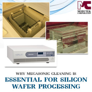
Adding Megasonic cleaning to standard wafer cleaning methods can reduce costs and improve overall semiconductor fabrication performance. Megasonic cleaning is especially useful for manufacturing silicon wafers with the smallest geometries, where almost complete particle removal is necessary for successful manufacturing. The process uses high-frequency sound waves to clean wafer surfaces and can be integrated into wet bench processing stations. Megasonic cleaning is becoming more essential for silicon wafer processing as product complexity increases.

Megasonic Cleaning Can Lower Costs

When Megasonic cleaning is incorporated into a silicon wafer processing line, lower costs can result from reduced chemical use and increased yields. The cleaning method uses only plain water in the cleaning bath and can be substituted for some chemical-based cleaning steps. For some cleaning applications, inexpensive solvents or mild detergents can be added to the cleaning solution. For example, Megasonic cleaning is often used after RCA clean to produce optimum cleaning results and reduce additional chemical usage.

When used with conventional cleaning methods, Megasonic cleaning results in cleaner wafers to reduce particle counts. Defects on the final semiconductor products are reduced. Yields increase because the reject rate is lower, and output quality increases.

How Megasonic Cleaning Reduces Particle Counts

Megasonic cleaning uses high-frequency sound waves to gently dislodge the smallest contaminating particles when wafers are emersed in a cleaning bath. During the last few years, several semiconductor manufacturers have been producing semiconductor devices that use 7 nm technology. Two leading-edge semiconductor manufacturers have recently done die shrinks to support the production of devices using 5nm and 3 nm processes. With increasingly close packing of semiconductor components, thinner conducting paths, and smaller structures, tiny contaminating particles on the wafer surfaces can block etching and cause component defects. The smaller geometries are especially sensitive to particles down to sub-micron size.

In the Megasonic cleaning process, a high-frequency generator produces an electric signal in the megahertz range. A transducer immersed in the cleaning solution converts the electric signal to sound waves. As the sound waves travel through the cleaning bath, they generate microscopic cavitation bubbles. The bubbles are formed in the sound wave troughs at low pressure and burst at sound wave high-pressure peaks. When a bubble bursts, it releases an energetic cleaning solution jet that strikes the wafer surface and cleans off contaminants. While the jet is powerful enough to remove foreign material from the wafer, it will not damage the underlying silicon.

Chemical cleaning methods effectively remove contaminants, but particles often remain on the wafer surface due to electrostatic and surface tension effects. The chemical action and rinsing are insufficient to remove many of the smallest particles. Megasonic cleaning and the action of the microscopic bubbles and jets dislodge these particles so that they can be rinsed away. The clean wafer is almost completely free of contaminating particles and ready for subsequent processing steps.

How Modutek Integrates Megasonic Cleaning into Semiconductor Manufacturing

While Megasonic cleaning improves cleaning performance throughout the semiconductor manufacturing process, low particle counts are especially critical for pre-diffusion cleans. Modutek has developed a complete line of wet bench stations designed and built using their in-house expertise. As a result, Modutek’s experts can advise customers on how to best integrate Megasonic cleaning in their process line and where it would be the most effective.

Modutek can also evaluate if a final Megasonic pre-diffusion cleaning step would improve process results and recommend additional Megasonic cleaning before critical etching steps. Fabrication with the smallest geometries will benefit the most from using Megasonic cleaning. When customers find that their particle counts at critical process steps are too high, Modutek can help find solutions using Megasonic technology.

Modutek Works with Customers to Provide Solutions

 As a leader in wet process semiconductor manufacturing equipment, Modutek works closely with customers to identify problems and provide innovative solutions. When customers need to upgrade their existing wafer cleaning process, Modutek can incorporate leading-edge technologies to improve wafer cleaning performance.