
- Home
- About Us
- Products
- Applications
- Support
- Blog
Improving Silicon Wafer Processing
Silicon wafer processing is the sequence of cleaning, etching, rinsing, drying, and film-forming steps that turns a bare silicon wafer into working semiconductor devices. Improving it means tightening control over uniformity, chemical delivery, temperature, and contamination at every step, because small variations at any stage can reduce yield, and the equipment running each step determines how well that control holds.
Process Engineers face many difficulties when processing silicon wafers, including maintaining uniformity across wafers and cleanliness while adhering to tight processing tolerances. Any misstep can result in yield losses that render wafers useless for device manufacturing. These complexities require precise controls, stringent safety protocols, and consistent maintenance.
Addressing Key Challenges
As semiconductor devices continue to shrink, the manufacturing margin of error becomes ever narrower.


This requires engineers to address various key challenges that include:
- Uniformity and Consistency: Ensuring uniform deposition or etching across a wafer is paramount. Non-uniformities could lead to device malfunction or decreased efficiency.
- Chemical Management: The semiconductor industry uses various chemicals with specific properties and reactions. Engineers must manage these reactions effectively to reach desired outcomes without introducing contaminants.
- Temperature Control: Many silicon wafer processing steps depend upon optimal temperature control. Maintaining the proper temperatures is critical to achieving the desired chemical reaction and physical properties.
- Defect Minimization: Any defect on a wafer, physical or chemical, could translate to malfunctioning or inefficient devices. The challenge is to minimize or eliminate these defects through meticulous processing.
Precision, Safety, and Maintenance
- Precision: For silicon wafer processing to succeed, everything from chemical deposition to physical etching must be conducted with unparalleled accuracy. This level of precision ensures the reliability and functionality of the final product.
- Safety: Wafer processing chemicals can be hazardous, so keeping personnel and the environment safe is paramount. This involves following strict safety protocols, using equipment with built-in safety features, and providing routine training.
- Maintenance: Equipment reliability is critical. Regular maintenance ensures longevity and keeps each process step consistent, minimizing variations that could affect wafer quality.


As technology advances, devices with smaller circuit geometries become increasingly demanding on wafer processing requirements. Minor variations that were once considered acceptable can now render devices unusable. As a result, this evolution necessitates creating even more precise process controls while pushing the boundaries of what is achievable.
Delivery and Measurement Requirements
In Silicon Wafer Processing, how chemicals and materials are delivered to the wafer can significantly impact the final result.
- Consistency: Delivering chemicals at regular intervals ensures that reactions proceed as anticipated, thus producing the desired layer thickness or etch depth.
- Accuracy: Precise measurements of chemical concentration or temperature ensure processes can be replicated consistently and reliably.
- Real-Time Monitoring: Because processes are so critical, real-time monitoring lets engineers make instant adjustments and address potential problems before they become severe.
Meeting these challenges requires cutting-edge equipment, refined processes, and skilled engineers. Overcoming these hurdles can yield significant rewards and pave the way for the next generation of electronic devices.
The Role of Equipment in Improving Wafer Processing Results
Reliable, user-friendly equipment is central to every successful silicon wafer processing operation. As technology advances, the need for sophisticated equipment and systems that deliver the required precision and consistency has become paramount. Here is why:
- Consistency: Reliable equipment ensures each processing step, from deposition to etching, is carried out uniformly across the wafer, leading to higher yield of functional semiconductor devices.


- Usability: User-friendly interfaces and controls let engineers focus on optimizing processes rather than wrestling with cumbersome equipment. This speeds processing and reduces the likelihood of human error.
The Edge of Innovative Equipment
Innovation is at the core of semiconductor manufacturing, and equipment must evolve with it. Innovative equipment provides:
- Adaptability: As device designs evolve and requirements change, adaptable equipment can quickly meet new demands, ensuring manufacturing continues smoothly.
- Efficiency: Cutting-edge equipment features advanced automation and monitoring, helping ensure processes are faster, more energy-efficient, and more resource-efficient.
Modutek's Wet Bench Systems Bridge Innovation and Reliability
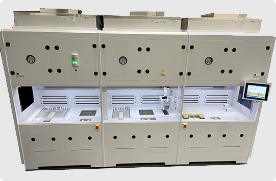
Modutek’s wet bench systems demonstrate how equipment can seamlessly combine reliability with cutting-edge innovations. Some notable features include:
- Megasonic Cleaning: This technology dramatically improves wafer-cleaning efficiency, producing a pristine wafer surface while reducing chemical use. This improves processing results and supports more eco-friendly operations.
- Ozone Cleaning:Modutek has pioneered an innovative new method for wafer cleaning. Ozone cleaning reduces water consumption by eliminating the need for wet chemical cleaners. This further reinforces Modutek's commitment to quality and sustainability.
- Ozone for Photoresist Removal: Modutek uses ozone for photoresist removal as an eco-friendly alternative to solvent strippers. This innovative method reduces the chemical footprint of wafer processing without impacting efficiency or productivity.


Equipment is more than just a tool; it plays a critical role in shaping silicon wafer processing quality, efficiency, and sustainability. Leveraging cutting-edge technologies such as those in Modutek’s wet bench systems helps manufacturers meet today’s and tomorrow’s challenges.
Cost-Effectiveness and Value
While initial costs of top-tier processing equipment might seem excessive, one must consider the bigger picture – the long-term value they bring. Investing in high-quality equipment provides several long-term advantages:
- Reduced Downtime: High-quality equipment breaks down less frequently, meaning fewer disruptions to production schedules and leading to consistent output.
- Higher Yield: Advanced equipment is designed to minimize errors and defects, increasing the percentage of usable silicon wafers. Over time, this increased yield can translate into significant cost savings and profits for your business.
- Longevity: High-quality equipment is built to last. This longer lifespan lets manufacturers defer significant replacement costs, improving returns on their initial investment.
How Modutek Delivers Cost-Effective Value
Modutek provides more than equipment; we deliver value. Here is how we do it:
- Customization: Realizing that one size doesn't fit all, Modutek offers customized equipment to support each customer's wet process requirements. This ensures customers aren't paying extra for features they don't need and have everything they need to optimize operations and save money.
- Ease-of-use: Modutek's equipment stands out for its user-friendly design. This shortens learning curves for new operators, ensures processes run with high precision, and minimizes costly errors.
- Reliability: Modutek's equipment uses high-quality materials and is designed to adhere to rigorous standards. This reliability ensures consistent performance day in and day out, maximizing productivity and profitability.


In semiconductor manufacturing, where margins can be thin and competition is fierce, every advantage counts. By providing cutting-edge, cost-effective equipment, Modutek ensures customers are well-equipped to succeed now and in the future.
Cleanliness and Chemical Compatibility
In silicon wafer processing, contamination can be the bane of productivity, leading to defects that compromise end-product performance and productivity. Recognizing the importance of cleanliness, Modutek’s wet bench stations are meticulously designed to incorporate the following:
- Prevent Contamination: Every aspect, from chemical flow and station structure to wafer-handling procedures, is designed to minimize the risk of contaminants contacting wafers.
- Ensure Seamless Chemical Flow: Modutek's stations ensure no residual mixture can contaminate subsequent processes by optimizing how chemicals are introduced and drained.
Ensuring Chemical Compatibility
Silicon wafer processing involves using a complex ballet of chemicals. These chemicals not only interact with the silicon wafer but also with the equipment used during processing. Modutek has developed methods to ensure chemical compatibility:
- Material Selection: Every material used to build wet bench stations must resist the chemicals commonly used in wafer processing. This prevents equipment degradation over time, which could introduce contaminants.
- Rigorous Testing: Before approval, materials undergo rigorous testing to ensure they can withstand prolonged chemical exposure without compromising integrity.
- Feedback Loop: Modutek continuously engages with process engineers and industry experts to gather feedback to ensure their equipment remains compatible with any new chemicals or processes introduced into the semiconductor manufacturing ecosystem.


Maintaining cleanliness and chemical compatibility is essential to silicon wafer quality. It also helps ensure the longevity of processing equipment. Modutek’s wet bench stations provide value to customers while simultaneously advancing industry standards.
Emphasizing Safety and Compliance
In the demanding environment of silicon wafer processing, where intricate procedures use potent chemicals with exact precision, safety is not just a priority; it’s imperative. Modutek recognizes this critical aspect by:
- Risk Reduction: Designing equipment that inherently reduces chemical-related hazards. This not only keeps operators safe but also extends equipment life to deliver consistent processing results.
- User-Friendly Design: By including intuitive controls and safety mechanisms, Modutek ensures that operators can complete procedures safely without undue risk, reducing the chance of human errors that could lead to safety breaches.
Compliance and Standards:
Compliance goes beyond simply ticking off boxes. It involves instilling safety and reliability into the DNA of every product. Modutek incorporates the following in its equipment:
- Broad-spectrum Compliance with Recognized Standards: Modutek's wet bench systems are designed and built to comply with various industry standards, including UL 508A, NFPA 70-NEC, NFPA 79, CSA CE Ashare. This ensures universal
- Optional Certifications: For organizations that require additional assurance or have specific needs, Modutek offers further testing and certifications, such as S8, S22, and IEC.EN, Structural PE, Seismic PE, and Title 22.
- Guaranteed Testing: Before delivery, all wet bench systems are rigorously tested using deionized water, reinforcing Modutek's commitment to delivering equipment that's not only functional but safe and reliable.


- Supporting Documentation: Recognizing the importance of transparency, Modutek provides comprehensive documentation attesting to the compliance of its equipment, ensuring customers can confidently integrate it into their operations.
Safety and compliance are integral parts of silicon wafer processing operations. Modutek’s unwavering dedication to these principles assures customers they are investing in top-tier equipment and partnering with a brand that prioritizes operator well-being and final-product integrity.
Maintenance and Customer Support
- Proactive Maintenance: Modutek aims to keep its equipment operating at peak levels by offering guidance on regular maintenance checks and servicing.
- Expert Support and Guidance: If any queries or concerns arise, Modutek's team of seasoned professionals is on standby to offer insight and help customers navigate challenges with confidence.
Beyond Warranty With Modutek Extended Service Contracts
Modutek understands that silicon wafer processing equipment may need extra support in a dynamic environment. To help customers overcome any such hurdles, Modutek offers extended support:
- Service Contracts: Besides providing standard warranty periods, Modutek offers customers the ability to enter service contracts that ensure priority service, timely updates, and regular equipment checks - keeping operations smooth and efficient.
- Customized Support: Every processing environment is unique. That is why Modutek service contracts are tailored to the customer's requirements, providing support that meets operational demands.


In silicon wafer processing, where precision is critical, equipment downtime or inefficiencies can cascade into reduced productivity and lower output quality. By providing reliable maintenance and customer support, Modutek ensures customers stay equipped to navigate these challenges and continue delivering outstanding results.
Ensuring Quality through Testing and Delivery
Designing and building state-of-the-art silicon wafer processing equipment is one thing, but ensuring it works flawlessly out of the box is another. That is why Modutek stands out in its commitment to quality assurance by providing the following:
- Factory Acceptance Testing (FAT): Every piece of equipment undergoes stringent FAT protocols. This comprehensive testing process is carried out under conditions that simulate real-world scenarios to ensure each unit performs optimally and meets Modutek's exacting standards.
- Deionized Water Testing: To guarantee purity and prevent potential contamination, all wet bench systems undergo thorough testing using deionized water. This step ensures the equipment can be quickly integrated into a customer's operations without risk to wafer quality.
- Meet Specific Requirements: Because every semiconductor facility has unique requirements, Modutek works closely with customers to ensure delivered equipment complies with operational needs and environment-specific demands.
Ensuring Seamless Transition Post-Delivery
Modutek goes beyond the factory when it comes to quality assurance:
- Installation and Integration: Since setting up complex equipment can be challenging, Modutek ensures seamless installation and integration into operational workflows.
- Customer Training and Guidance: To help customers make the most of their investment, Modutek provides detailed training sessions, ensuring staff can operate the equipment confidently and efficiently, maximizing its potential and lifespan.
Processing silicon wafers requires precision, reliability, and consistency. Modutek’s rigorous pre-delivery testing and post-delivery support ensure customers receive top-quality equipment and can use it to its full potential for optimal results every time.

Leveraging Data for Improved Results
Data is the lifeblood of manufacturing operations, offering insights that can drive process optimization, efficiency gains, and, ultimately, better results. Silicon wafer processing operations benefit immensely from reliable, trackable data.
- Real-Time Data Acquisition: Modutek's semi-automated wet process and automated wet bench systems record key operational metrics in real time, continuously. This allows process engineers to make immediate adjustments when needed and ensures a holistic understanding of the entire process.
- Historical Data Analysis: Modutek's systems enable users to quickly analyze past data for trends and potential issues while fine-tuning processes. This historical insight is invaluable for proactive troubleshooting and continuous improvement initiatives.
- Integration With Operational Software: Recognizing that silicon wafer processing does not happen in isolation, Modutek's systems are designed to integrate with broader operational software infrastructures. This ensures that data from wet bench systems can be easily combined with other datasets for an in-depth view of the entire production cycle.
- Enhancing Accountability and Traceability: Modutek's systems enhance accountability by keeping a detailed operations log. Whether tracking the efficiency of specific batches, monitoring equipment performance, or tracing potential anomalies, data-driven insights ensure decisions are based on solid evidence.
When utilized effectively, data can be a game-changer, turning challenges into opportunities and inefficiencies into optimizations. Modutek’s cutting-edge systems equip process engineers and facility managers with top-tier silicon wafer processing equipment and analytical tools necessary to push the boundaries of what is possible in the semiconductor industry.


The Bottom Line
Silicon wafer processing requires a careful balance between precision, reliability, and efficiency. The choice of equipment and the supplier can significantly affect the final product’s quality, consistency, and production costs.
Factors to Consider When Buying Wafer Processing Equipment
- Track Record: Consider the history and reputation of the equipment manufacturer. Have they consistently delivered quality solutions to the industry?
- Customization: Each semiconductor manufacturing and R&D facility has unique requirements. Can your chosen supplier offer tailored solutions that align seamlessly with these operational demands?
- Customer Support & Maintenance: Longevity and efficiency of equipment often depend upon the quality of support and maintenance that follows after purchasing equipment.
Modutek: A Legacy of Excellence
With over 40 years in the business, Modutek exemplifies uncompromising quality, innovation, and customer commitment. Modutek’s track record–from tailored equipment solutions to repeat business from satisfied customers–speaks volumes about our commitment to excellence within the semiconductor industry.
Whether you are a process engineer, R&D professional, or facility manager, partnering with Modutek will elevate your silicon wafer processing operations. Contact Modutek for a free consultation to discuss your specific silicon wafer processing requirements.

FAQs About Silicon Wafer Processing
What Causes Yield Loss During Silicon Wafer Processing?
Yield loss in wafer processing commonly traces back to contamination and process variation. Particles on the wafer surface, metallic impurities such as iron and aluminum, organic residues, and uneven etching or cleaning across the wafer all create defects that degrade device performance. Controlling chemical purity, temperature, and rinse and drying quality at each step keeps these sources in check.
How Does Temperature Control Affect Etch Rate Consistency?
Wet etch rates change with bath temperature, so small temperature drift shows up directly as variation in etch depth. Anisotropic silicon etching in KOH, for example, follows an Arrhenius-type temperature dependence, which means a few degrees of drift can noticeably change the etch rate. Adding circulation or some type of agitation to the process will help stabilize the process temperature.