Experts in Wet Process Equipment,
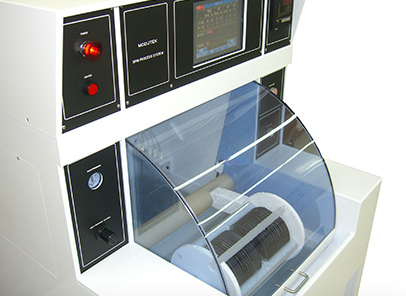
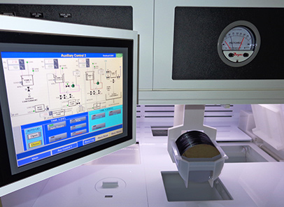
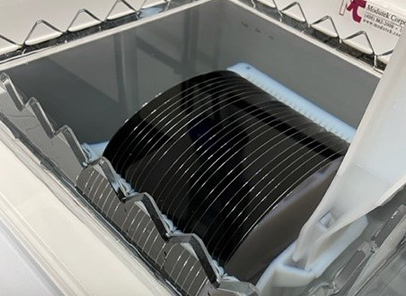
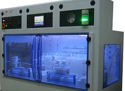
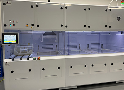
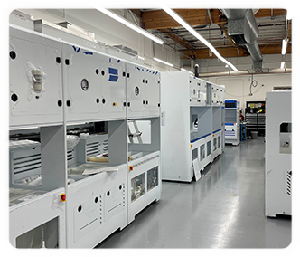
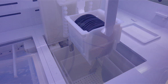
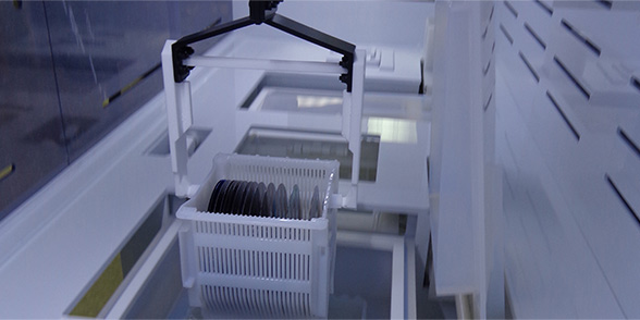
Wet Bench Design and Manufacturing
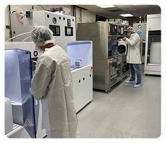
Wet Bench Design and Manufacturing
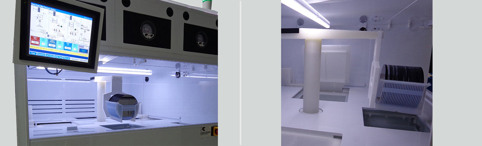
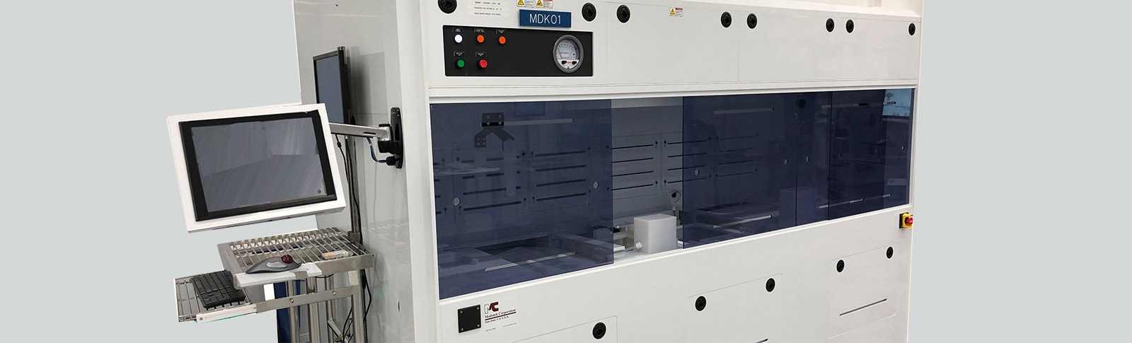
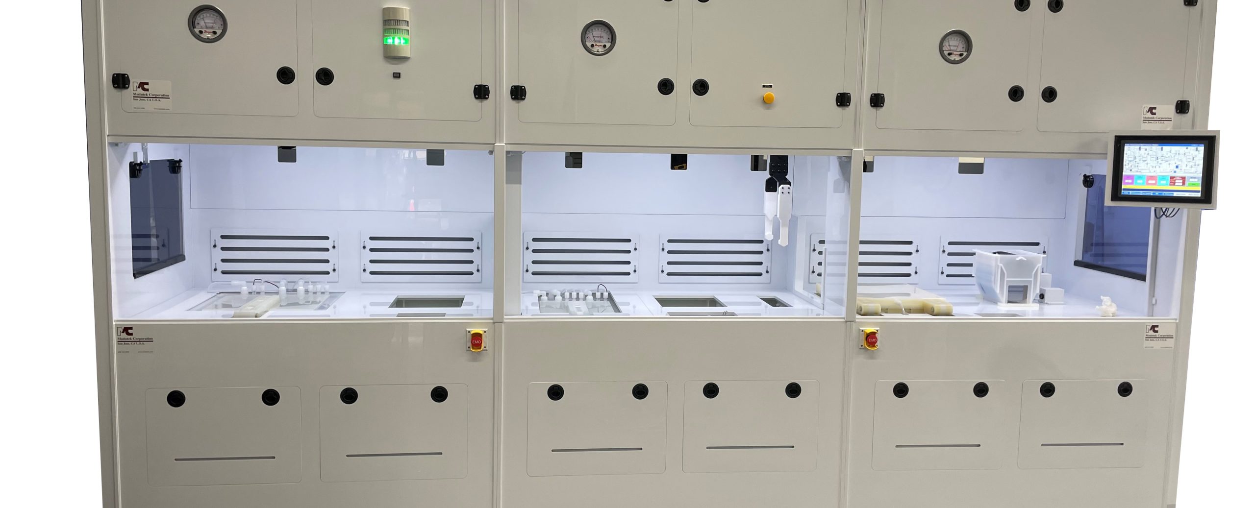
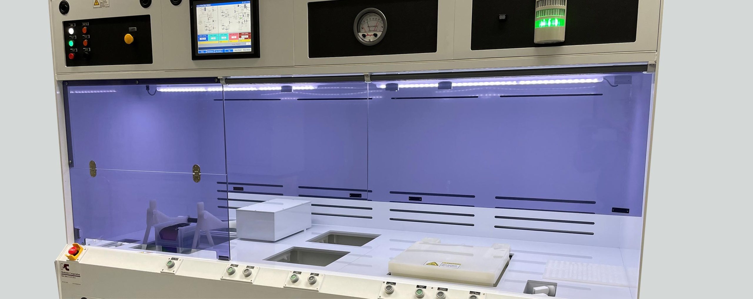
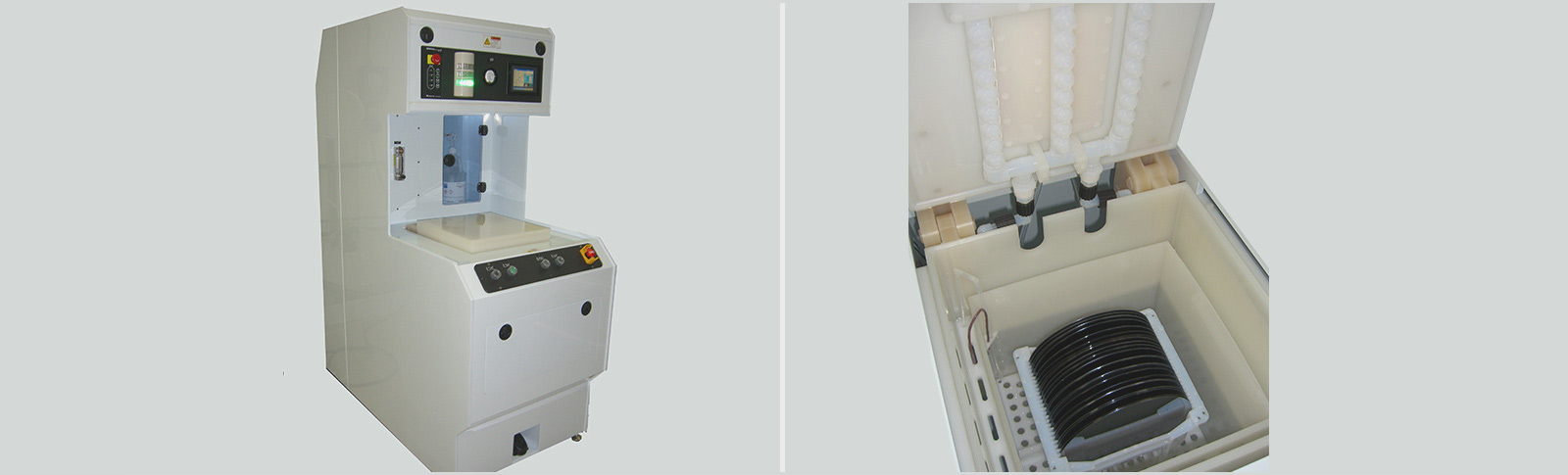
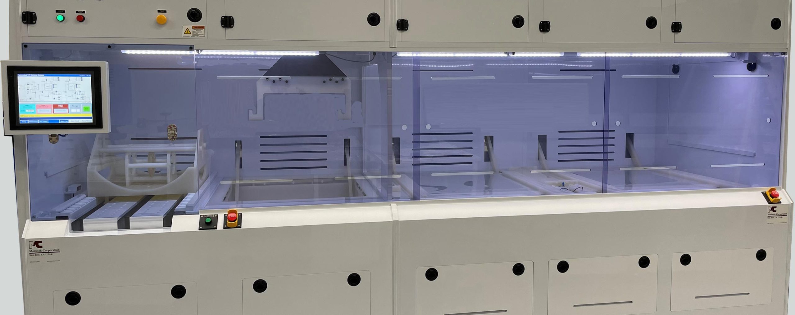
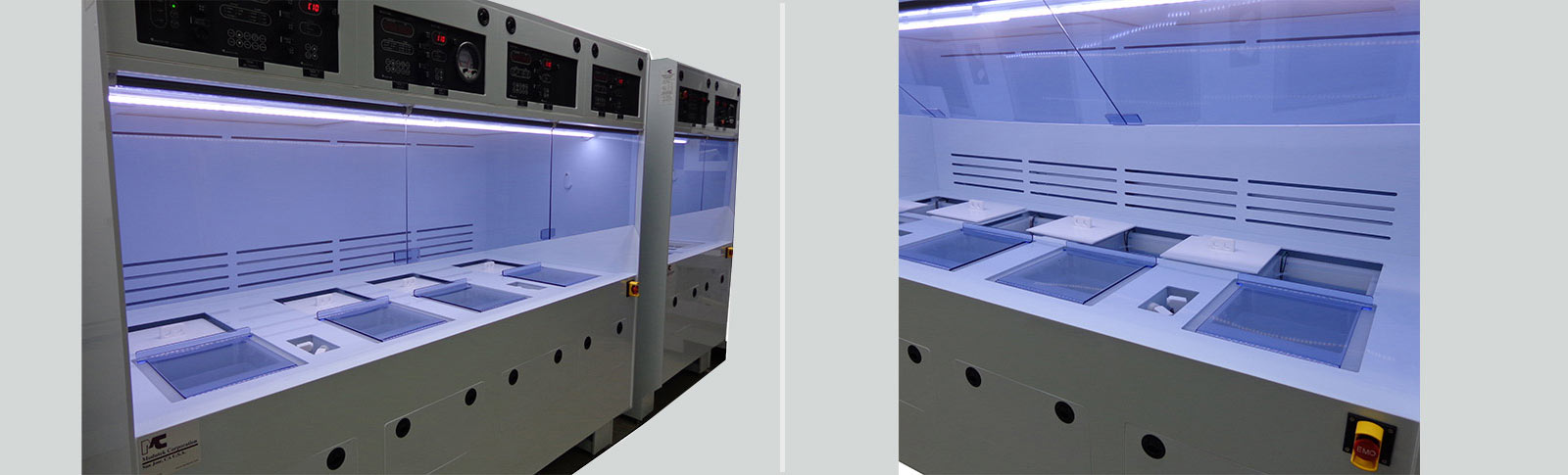
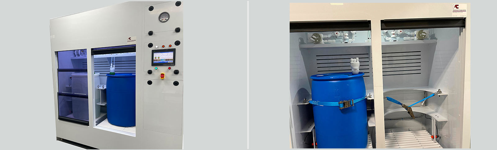
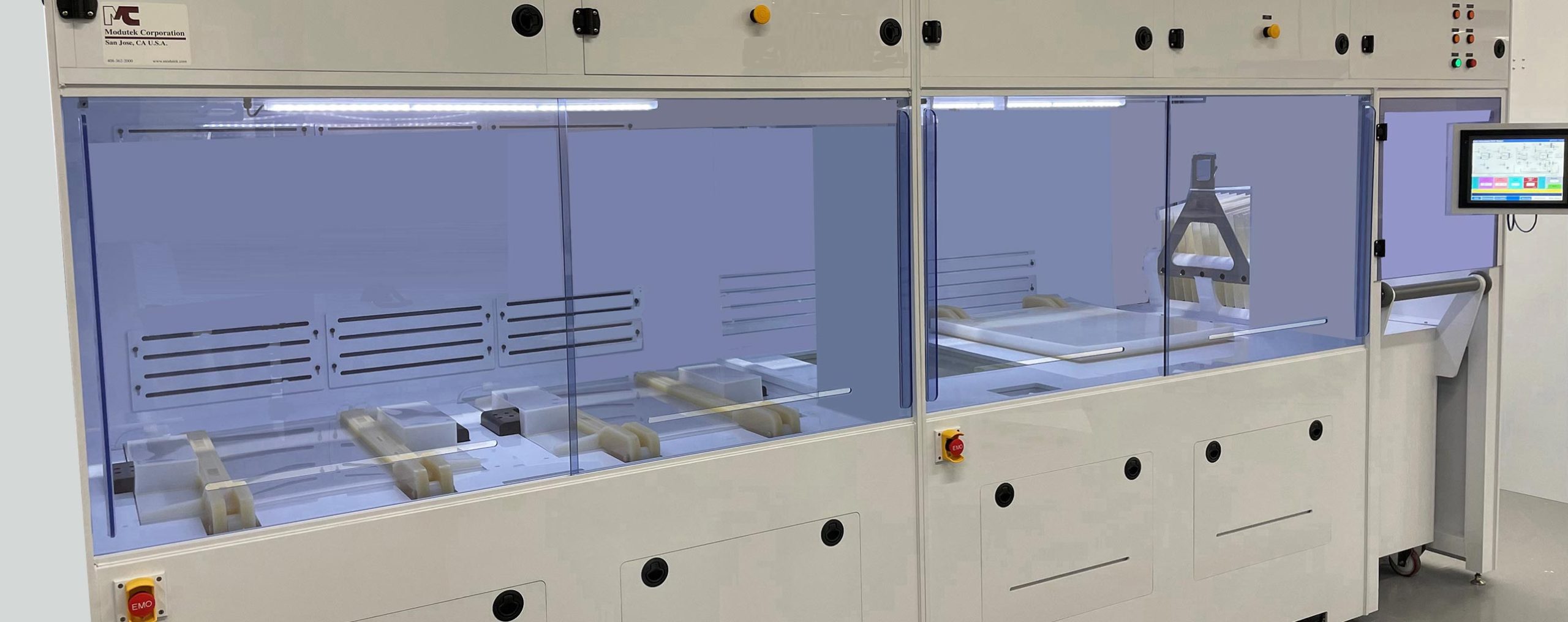
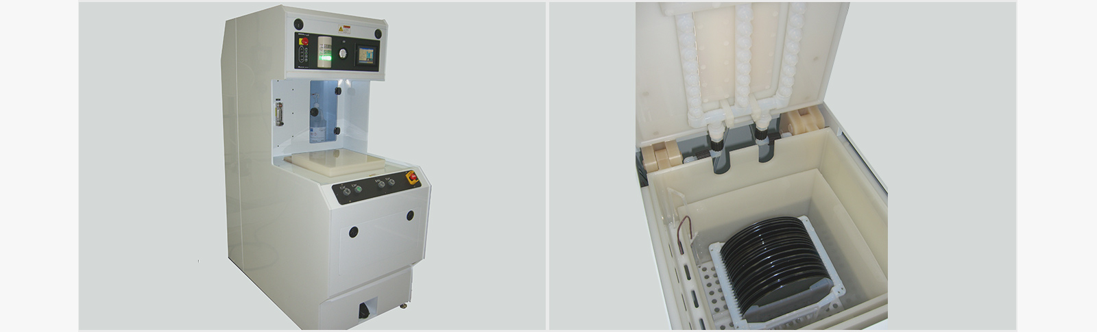
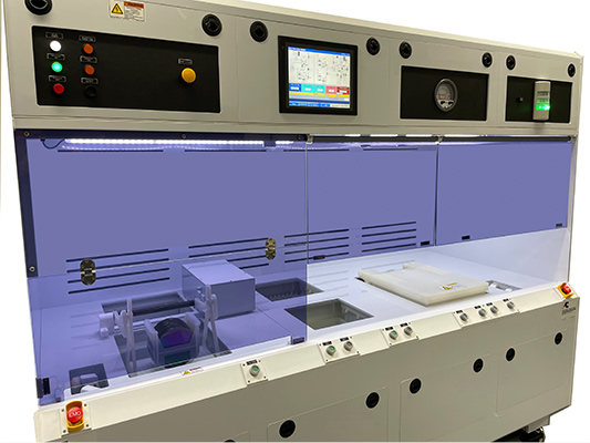
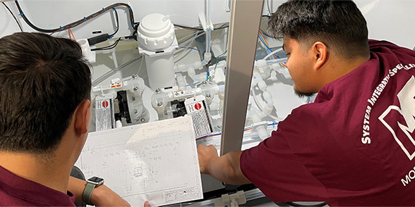
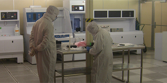
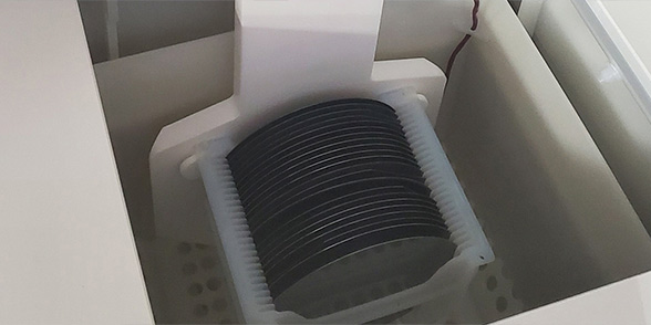
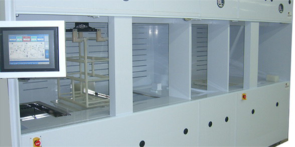
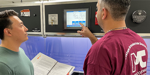

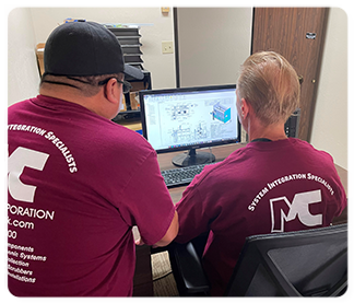
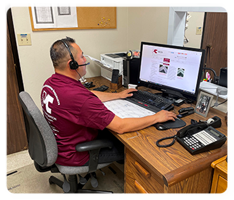
In-house engineering experts, state-of-the-art technology, and end-to-end fabrication capabilities are all designed and built into Modutek’s systems to ensure quality, high reliability, direct customer support.

Modutek has been providing equipment and systems to meet the needs of technology customers continuously for over 40 years.