Silicon Wafer Cleaning: Removing Contaminants to Improve Yields
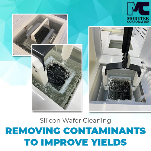
Editor’s Note: This article was originally published in April 2016 and has been updated with new information and re-posted in February 2024. In the intricate world of semiconductor manufacturing, the cleanliness of silicon wafers is not just a requirement; it’s a critical success factor. Each wafer must undergo many processing steps requiring rigorous cleaning to […]
Why Megasonic Cleaning is Essential for Silicon Wafer Processing
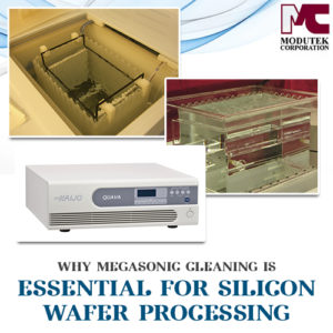
Adding Megasonic cleaning to standard wafer cleaning methods can reduce costs and improve overall semiconductor fabrication performance. Megasonic cleaning is especially useful for manufacturing silicon wafers with the smallest geometries, where almost complete particle removal is necessary for successful manufacturing. The process uses high-frequency sound waves to clean wafer surfaces and can be integrated into […]
How the IPA Vapor Dryer Improves Wafer Processing Results
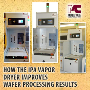
Not every advancement in semiconductor fabrication produces results that are usable in industry. To be of value, advancements need to be consistently repeatable when used on an industrial scale. Modutek’s IPA vapor dryer falls into this category, helping semiconductor fabricators improve both yields and processing times. Modutek’s IPA vapor dryers are custom-engineered with in-house experts […]