- Home
- About Us
- Products
- Applications
- Support
- Blog
- Home
- About Us
- Products
- Applications
- Support
- Blog
Wafer Etching Process
KOH Etching
The etching of silicon wafers with potassium hydroxide (KOH) creates microscopic structures in the silicon. The etching rate is controlled by the temperature of the etching bath, the concentration of KOH, and the crystalline structure along with any impurities in the silicon wafer. KOH etching provides a low-cost and repeatable etching process that etches quickly. Modutek improves KOH etching applications using either the TFa or TT series of PFA Teflon tanks. For more details refer to the article “Improving the KOH Etching Process Using Teflon Tanks“.
Buffered Oxide Etch (BOE)
BOE is also known as buffered HF or BHF and is primarily used in etching thin films of silicon nitride or silicon dioxide. It consists of hydrofluoric acid and a buffering agent such as ammonium fluoride. BOE provides a consistent repeatable process, does not undercut masked oxide, does not contaminate or stain diffused silicon surfaces, and is compatible with photoresist. Modutek supports the BOE process specifically with the F SERIES sub-ambient filtered etch bath.
Silicon Nitride Etching
Silicon nitride is used as a masking material in semiconductor manufacturing. It is deposited on the silicon wafer as a thin film and is etched with hot phosphoric acid. In a nitride etch bath, a hot phosphoric acid strip is performed at 180 degrees C. Nitride etch baths provide precise temperature control by regulating the de-ionized water to phosphoric acid ratio. Modutek’s silicon nitride etch baths provide accurate process control with consistent repeatability and high safety. For more details on process control and safety refer to the article “Safely Controlling the Silicon Nitride Etching Process“.
Copper, Gold, and Aluminum Etching
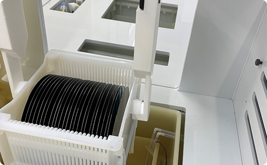
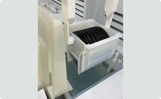
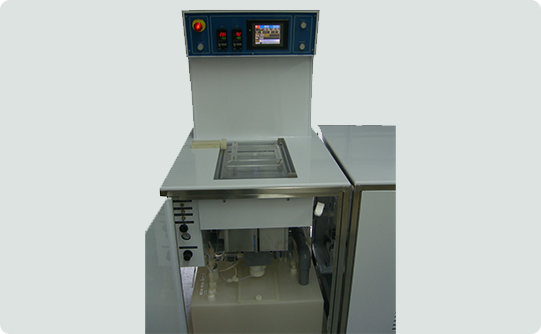
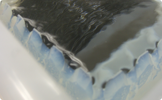
Microelectronic devices developed on silicon wafers must use metallic connections to conduct electric signals. Metals used for this purpose include aluminum, copper, or gold, which are deposited on the silicon wafer. Some of the metals will need to be etched during the silicon wafer fabrication process. Etching metals can be challenging; effective etching relies on selecting the appropriate chemicals and process. In these cases, using Modutek’s Vacuum Metal Etcher provides a precise process for etching metal layers. Wafers are etched within a vacuum so that hydrogen bubbles, an etching reaction that causes “snow” and “bridging,” are immediately removed from the surface of the wafer. An evacuating pump in the Vacuum Metal Etcher directly exhausts the hydrogen bubbles. Modutek’s equipment can use various etchant solutions to etch different metals.
Modutek Support for Wafer Etching Process Applications
Modutek has been a premier supplier of semiconductor manufacturing equipment for over 40 years and has a full line of wet processing equipment to support a wide variety of wafer etching process applications. The equipment that Modutek provides delivers reliable and repeatable results safely and accurately. Contact Modutek for a free quote or consultation on selecting the right equipment for your process requirements.