 Research and development (R&D) in the semiconductor industry requires precision and accuracy and the adaptability that customized equipment provides. When seeking to innovate or refine existing semiconductor technologies, R&D professionals often encounter unique challenges that cannot adequately be addressed with off-the-shelf equipment. This is where supporting unique wafer processing applications with customized equipment becomes indispensable.
Wafer processing equipment is at the core of semiconductor R&D labs, providing experimental processes and rapidly changing requirements with sufficient flexibility. For example, developing new semiconductor materials or device structures often requires modifications to standard etching, cleaning, and deposition techniques. Customized equipment enables researchers to tweak these processes in real-time, speeding up experimental phases and decreasing time-to-market for new technologies.
Modutek’s wafer processing equipment blends customization with precision engineering. By designing equipment to meet the specific needs of technology manufacturers, Modutek provides solutions tailored specifically for various R&D activities. This includes adjustable chemical delivery systems, temperature controls, and wafer processing automation levels. Ensuring that each piece of equipment conforms to the precise specifications of any given project provides greater flexibility. This flexibility enhances the capabilities of R&D teams while meeting the economic demands of the semiconductor industry, where the efficiency of research processes directly impacts production costs and development speed.
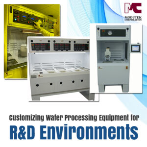
Tailored Solutions for Varied R&D Needs
In R&D, the diversity of projects often requires equipment that can adapt to a wide range of specifications and processes. Modutek’s wafer processing equipment excels in this regard by offering highly customizable solutions. This adaptability is vitally important to laboratories working at the forefront of semiconductor research and development where standardized equipment may fall short.
R&D laboratories benefit greatly from features like programmable controls and modular system designs. These systems enable rapid reconfigurations for different types of wafer processing tasks ranging from etching to cleaning to deposition. This caters to the ever-evolving needs of research projects. Modutek’s systems are specifically engineered to allow seamless transitions between various operational modes to maximize lab efficiency and throughput.
Customizing tools to specific parameters allows R&D teams to experiment with novel processes and materials without being constrained by traditional production-focused equipment. This flexibility enhances experimental outcomes while promoting faster innovation to meet market needs.
Key Features of Customizable Wafer Processing Equipment
Modutek’s wafer processing equipment is designed with several key features to meet the stringent demands of R&D environments:
- Precision Control: Advanced control systems provide precise process parameter adjustments to develop new semiconductor technologies. This high level of control provides consistency and accuracy in research outcomes.
- Flexibility: The equipment’s modular design facilitates quick reconfiguration, accommodating diverse processes such as etching, deposition, and cleaning. This flexibility is essential for labs that must rapidly switch between research protocols.
- Reliability: Modutek’s systems are built for durability and consistent performance to withstand the rigorous demands of continuous R&D operations. Reliable equipment reduces downtime and maintains continuous workflow.
- Versatility: These systems can support a wide range of R&D activities with customizable options. Versatility extends to handling different wafer sizes and types, which is vital for labs working on diverse semiconductor applications.
- Customization Options: Equipment, from chemical delivery systems to temperature settings, must be customized to meet the project-specific needs of R&D professionals. This ensures that R&D professionals can adapt the equipment to the project’s needs without compromise.
Tailoring Solutions to Specific Processes
In semiconductor R&D, each process has unique requirements that demand tailored solutions. Modutek’s customizable wafer processing equipment excels at meeting these needs by offering specific adaptations for various semiconductor fabrication processes:
- Etching: Customizable settings allow precise control over etching chemicals and techniques, which is crucial for accurate pattern fidelity.
- Deposition: Equipment can be adjusted for optimal temperatures and deposition rates to produce uniform layers with minimum defects.
- Cleaning: Configurations can be modified to optimize cleaning effectiveness, which is critical to wafer purity and performance.
- Integration and Compatibility: Modutek’s systems are engineered to integrate seamlessly with existing setups, enhancing overall process efficiency and ensuring compatibility.
These tailored solutions help researchers achieve optimal results in each specific process, pushing the limits of semiconductor technology forward.
Expanding Capabilities with Advanced Technology
Modutek’s wafer processing equipment increases efficiency and opens up a range of research possibilities. Leveraging advanced technology enhances efficiency and enables new research possibilities.
- Automated Process Controls: These controls enhance process consistency and reduce manual intervention, which allows researchers to focus on innovation instead.
- Data Integration: Systems designed to collect and analyze process data provide invaluable insights, helping to refine methods and enhance outcomes.
- Scalability: Equipment can be scaled to meet the demands of both small-scale experiments and larger production trials, offering flexibility as project scopes grow.
Modutek’s equipment, which incorporates advanced technologies, assists semiconductor professionals in pushing the limits of current technology while exploring future possibilities.
The Bottom Line
In semiconductor manufacturing, the ability of equipment to support unique wafer processing applications to meet the needs of R&D is invaluable. Modutek’s equipment and systems are designed with flexibility in mind to support integration into any research environment. This flexibility ensures that each setup meets immediate project needs while remaining adaptable as research directions change over time.
By investing in Modutek’s customized wafer processing solutions, R&D labs can significantly increase operational efficiency and throughput while remaining at the forefront of technological innovations. Contact Modutek for a free consultation to discuss your R&D equipment needs.