 When silicon wafers are cleaned between manufacturing steps, it is critical to remove all contamination from the wafer surfaces. The remaining traces of process chemicals or microscopic particles can disrupt the etching process and result in defective or low-quality semiconductor devices.
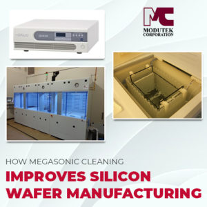
Megasonic cleaning uses high-frequency sound waves in the cleaning tank to remove contaminants and particles from the silicon wafers. The technology can save time and money because it works quickly and does not require expensive chemicals. Silicon wafers cleaned with Megasonic cleaning are completely clean with a reduced particle count. As a result, the technology can improve the operation of semiconductor manufacturing lines for semiconductor fabricators and research labs.
Megasonic Cleaning Reduces the Use of Toxic Chemicals
The cleaning of silicon wafers after the completion of each semiconductor manufacturing step is accomplished by soaking the wafers in mixtures of chemicals including hydrochloric acid or sulfuric acid. In addition to the cost of the chemicals themselves, there are ongoing costs related to the storage, delivery, and disposal of these chemicals. The possibility of leaks and the disposal of the waste chemicals represent environmental hazards that are continuously being mitigated with tighter regulations. Reducing the use of aggressive chemicals can save money beyond their direct cost and can improve the environmental footprint of the semiconductor manufacturing facility.
With Megasonic cleaning, a frequency generator produces an electric signal in the MHz range that is transmitted to a transducer. The transducer that is immersed in the cleaning solution converts the signal to sound waves in the cleaning tank. The sound waves create microscopic cavitation bubbles that deliver a gentle scrubbing action against the surface of the silicon wafer. The cleaning intensity is strong enough to dislodge impurities and contaminants but will not damage the wafer surface or the microscopic structures that have been etched into it.
When Megasonic cleaning is used to replace some of the traditional cleaning steps, the use of chemicals is reduced. Megasonic cleaning uses plain water or water with the addition of mild detergents. The cost benefits and reduced environmental impact can be substantial, and the areas where Megasonic cleaning is used will have increased worker safety and reduced chemical exposure.
Megasonic Cleaning Can Deliver Improved Cleaning Performance
While acid baths work well for cleaning general contaminants from silicon wafer surfaces, ensuring low particle counts can be challenging. Contaminating particles can block etching and cause defects in the final semiconductor devices. As functions become more and more closely packed on the wafer and microscopic structures become smaller, a single particle can affect the etched shapes and current paths. A key factor for improving output quality and reducing defects is reducing particle counts to a minimum.
Microscopic particles can be difficult to remove from the surface of silicon wafers because they often develop a static charge that allows them to cling to the wafer. Chemicals can dissolve the substances that make the particle adhere to the wafer surface but the static charge often remains as an additional bond. With Megasonic cleaning, very small cavitation bubbles form and collapse in tune with the sound wave frequency in the MHz range. When a bubble collapses near the wafer surface, it emits a powerful jet that dislodges any particle still clinging to the surface. Wafers that have been cleaned with Megasonic cleaning systems have a lower particle count as well as a high degree of cleanliness.
Modutek Can Help with Megasonic Cleaning Integration
As a leading manufacturer of wet process semiconductor manufacturing equipment, Modutek can help customers integrate Megasonic cleaning into their wafer cleaning process. Modutek offers free consultation and can show customers how to realize the benefits of lower costs, better output quality, and improved yields.