 During silicon wafer processing, impurities and particles are deposited on wafer surfaces or are left over from previous process steps. Such particles can cause defects in the final semiconductor product. With the reduced size of today’s silicon wafer microstructures, even the tiniest particles can block etching and affect the diffusion processes. The result appears in the final semiconductor circuit as either as a defect or reduce quality and life expectancy of the product. As a result, the focus of many wafer cleaning operations is to leave the silicon wafer surface intact but free of contaminating particles.
How Particles are Removed from Silicon Wafer Surfaces
The removal of particles can be difficult because they often have a chemical or electrostatic affinity for the silicon surface. They are attracted to the silicon wafer because of electrostatic charges and specific mechanisms have to be used to dislodge and remove them. The smaller the particle, the more such attraction may play a role and the harder it is to remove every particle from the wafer.
Mechanisms to remove particles include silicon wafer cleaning with a chemical that reacts with the particles, cleaning with a solution that dissolves the particles or washing the particles from the wafer surface. In each case, a specific type of equipment is required and traditional standard processes can be used together with new technologies aimed at removing even the smallest particles.
Cleaning Processes
Many chemical processes used to clean silicon wafers have remained unchanged since they were first used 30 years ago. These methods use aggressive chemicals to remove contamination from the wafers, which are then rinsed with de-ionized water and dried. These methods remove most of the contaminants but are less effective in removing the smallest particles. Refined older methods and new technologies such as megasonic cleaning are now often used to complete the cleaning process.
Cleaning methods used at different stages of the silicon wafer fabrication process include the following:
- The RCA clean process, often carried out in two steps called SC1 and SC2, prepares a wafer for further processing. SC1 cleans wafers with a mixture of ammonium hydroxide and hydrogen peroxide to remove organic residue. SC2 uses hydrochloric acid and hydrogen peroxide to remove metallic residues and particles.
- The Piranha cleaning process removes large amounts of organic residue such as photoresist. It uses sulfuric acid and hydrogen peroxide in a particularly corrosive mixture that acts quickly but must be handled with care.
- Megasonic cleaning dislodges particles and other contaminants using microscopic cavitation bubbles generated by a megasonic cleaning system. The bubbles form and collapse in time with the MHz sound waves, delivering a scrubbing action that overcomes particle attraction to the silicon wafer surface.
- The Ozone cleaning process uses ozone to convert organic particles and contaminants to carbon dioxide. All organic traces on a wafer surface are completely removed, leaving the silicon wafer free from particles.
One of the most critical processes for silicon wafer cleaning is the pre-diffusion clean process that takes place just before the wafers are placed in the diffusion oven. Any of the above methods or a combination of cleaning methods can be used to ensure that wafers are free of particles and the diffusion will be even and consistent.
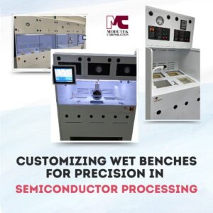
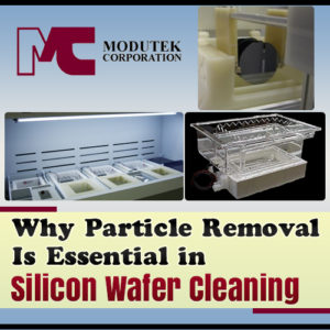
Equipment Used for Wafer Cleaning
Modutek’s wet bench technology supports all the above cleaning methods and can be provided within their manual, semi-automated or fully automatic systems. The company can offer equipment for traditional cleaning and for the new megasonic and ozone methods as well. All cleaning equipment is available in standard configurations but Modutek can also design custom products to meet the needs of any of their customers’ silicon wafer cleaning requirements. If you need highly reliable equipment to support your semiconductor manufacturing processes call Modutek for a free consultation or quote at 866-803-1533 or email Modutek@modutek.com.